Porpoise Purpose Module
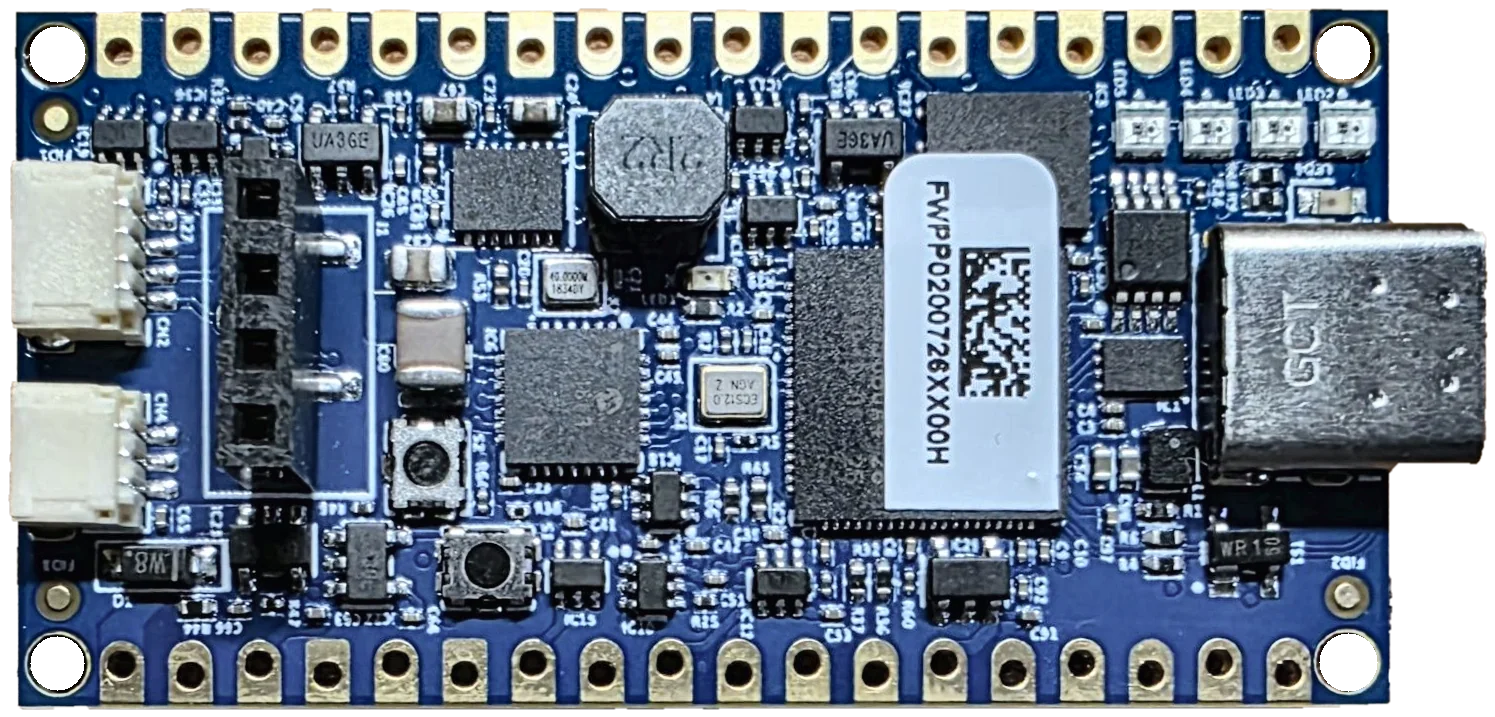
The Porpoise Purpose Module (PP Module) is a small FREE-WILi board for embedded control and bench work. It has CAN FD, UART, SPI, I²C, GPIO, an analog input, microSD storage, switchable power outputs and battery support, all on a 51 × 26 mm module with castellated edge pads.
It runs the same FREE-WILi firmware family as FREE-WILi 2. That means the same serial console, the same menu commands, the same OneWili API and the same rThon and WiliWasm scripting. Code you write for one board works on the other wherever the hardware matches.
A CAN FD node on your desk, a level-shifted UART / SPI / I²C adapter, a scripted test fixture, or a building block soldered into your own carrier board.
At a glance
- CAN FD: one channel with an on-board transceiver and software-switchable 120 Ω termination.
- Buffered I/O: 13 signals (UART, SPI, I²C, GPIO) behind level shifters. You choose the logic level with IO VREF, from 1.8 V to 5 V.
- 3.3 V I/O: a Qwiic I²C bus (I2C1) and a 0–3.3 V analog input.
- Power outputs: 3.3 V and 5 V outputs, plus four switchable power zone outputs you control from software.
- Battery: single-cell 3.7 V Li-ion / LiPo support, with on-board charging and protection.
- Storage: 16 MB flash, 8 MB PSRAM and a microSD card slot.
- Extras: four addressable RGB LEDs, a header for an optional I²C OLED display, BOOT and RESET buttons, and a 3-pin SWD debug connector.
- USB-C for power, the serial console and firmware updates.
- Mounting: 36 castellated pads at a 2.54 mm pitch. Solder them to a carrier board, or press standard headers in for temporary use.
Specifications
| Processor | 150 MHz dual-core microcontroller |
| Memory | 16 MB flash · 8 MB PSRAM · microSD card slot (4-bit SD) |
| USB | USB-C, USB 2.0 Full Speed. Serial console (CDC), power and firmware updates |
| CAN | 1 × CAN FD, on-board transceiver, switchable 120 Ω termination |
| UART | 1 × UART with RTS/CTS, buffered (pins 8–11) |
| SPI | 1 × SPI controller, buffered (pins 14–17) |
| I²C | I2C0: buffered, pins 4–5 · I2C1: 3.3 V, on the Qwiic connector, the display header and pins 29–30 |
| GPIO | 13 buffered GPIO (logic level = IO VREF) plus 2 × 3.3 V GPIO. PWM on any buffered GPIO |
| Analog | 1 × analog input, 0–3.3 V |
| LEDs | 4 × on-board addressable RGB LEDs. Up to 3 external LED strips on GPIO25 / GPIO26 / GPIO27 |
| Power in | USB-C 5 V, or a single-cell 3.7 V Li-ion / LiPo battery |
| Power out | 3.3 V (1 A rail, shared with the module) · 5 V (2 A rail, shared) · 4 × switched IO VREF power zones |
| Battery charging | 220 mA from USB, with over-charge and over-discharge protection |
| Size | 51.00 × 26.00 mm |
| Mounting | 4 × Ø2.20 mm holes · 36 castellated pads, 2.54 mm pitch |
| USB IDs | VID 0x093C, PID 0x2061 |
Pinout
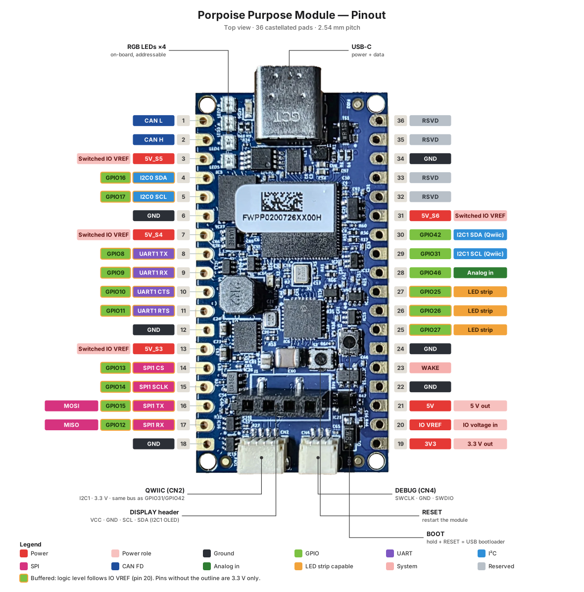
Pins are numbered counter-clockwise from pin 1, at the top-left next to the USB-C connector. Pins 1–18 run down the left edge and pins 19–36 run up the right edge. Pin names match the FREE-WILi 2 20-pin GPIO header (UART1 TX, SPI1 CS, I2C0 SDA, GPIO25 …), and the GPIOxx numbers are the ones the console and the API use: i\g\s 25 drives GPIO25 (pin 27).
Pins with an orange outline in the diagram are buffered. Their logic level follows IO VREF (pin 20). All other signal pins are 3.3 V only.
Pin descriptions
| Pin | Name | GPIO | FREE-WILi 2 pin | Logic level | Description |
|---|---|---|---|---|---|
| 1 | CAN L | — | 16 | — | CAN FD bus low. Switchable on-board 120 Ω termination. |
| 2 | CAN H | — | 18 | — | CAN FD bus high. |
| 3 | 5V_S5 | — | — | — | Power zone output. Switched copy of IO VREF (zone 6). |
| 4 | I2C0 SDA | GPIO16 | 10 | IO VREF | Buffered I²C data. Pulled up to IO VREF. Needs IO VREF of 3.3 V to 5.5 V. |
| 5 | I2C0 SCL | GPIO17 | 8 | IO VREF | Buffered I²C clock. Pulled up to IO VREF. Needs IO VREF of 3.3 V to 5.5 V. |
| 6 | GND | — | 19 / 20 | — | Ground. |
| 7 | 5V_S4 | — | — | — | Power zone output. Switched copy of IO VREF (zone 5). |
| 8 | UART1 TX | GPIO8 | 9 | IO VREF | Buffered. Default output. |
| 9 | UART1 RX | GPIO9 | 5 | IO VREF | Buffered. Default input. |
| 10 | UART1 CTS | GPIO10 | 7 | IO VREF | Buffered. Default input. |
| 11 | UART1 RTS | GPIO11 | 11 | IO VREF | Buffered. Default output. |
| 12 | GND | — | 19 / 20 | — | Ground. |
| 13 | 5V_S3 | — | — | — | Power zone output. Switched copy of IO VREF (zone 4). |
| 14 | SPI1 CS | GPIO13 | 1 | IO VREF | Buffered. SPI chip select. Default output. |
| 15 | SPI1 SCLK | GPIO14 | 15 | IO VREF | Buffered. SPI clock. Default output. |
| 16 | SPI1 TX | GPIO15 | 13 | IO VREF | Buffered. SPI data out (MOSI). Default output. |
| 17 | SPI1 RX | GPIO12 | 12 | IO VREF | Buffered. SPI data in (MISO). Default input. |
| 18 | GND | — | 19 / 20 | — | Ground. |
| 19 | 3V3 | — | 6 | — | 3.3 V output. On whenever the module is running. |
| 20 | IO VREF | — | 4 | — | I/O reference voltage input. Sets the logic level of every buffered pin. Connect to 3V3 (pin 19), 5V (pin 21) or an external 1.8 V to 5.0 V supply. Buffered pins are disabled while IO VREF is unpowered. |
| 21 | 5V | — | 2 | — | 5 V output. On by default (zone 1). Also powers the CAN transceiver. |
| 22 | GND | — | 19 / 20 | — | Ground. |
| 23 | WAKE | — | — | 3.3 V | Wake input. Drive high (3.3 V max) to wake the module from low-power sleep. |
| 24 | GND | — | 19 / 20 | — | Ground. |
| 25 | GPIO27 | GPIO27 | 3 | IO VREF | Buffered. Default output. Can drive an addressable LED strip. |
| 26 | GPIO26 | GPIO26 | 14 | IO VREF | Buffered. Default input. Can drive an addressable LED strip. |
| 27 | GPIO25 | GPIO25 | 17 | IO VREF | Buffered. Default output. Can drive an addressable LED strip. |
| 28 | GPIO46 | GPIO46 | — | 3.3 V | Analog input. 0 V to 3.3 V. Not buffered: 3.3 V logic only. |
| 29 | GPIO31 | GPIO31 | — | 3.3 V | I2C1 clock: the same bus as the Qwiic connector and the display header. Not buffered: 3.3 V logic only. |
| 30 | GPIO42 | GPIO42 | — | 3.3 V | I2C1 data: the same bus as the Qwiic connector and the display header. Not buffered: 3.3 V logic only. |
| 31 | 5V_S6 | — | — | — | Power zone output. Switched copy of IO VREF (zone 7). |
| 32 | RSVD | — | — | — | Reserved for factory use. Leave unconnected. |
| 33 | RSVD | — | — | — | Reserved for factory use. Leave unconnected. |
| 34 | GND | — | — | — | Ground. |
| 35 | RSVD | — | — | — | Reserved for factory use. Leave unconnected. |
| 36 | RSVD | — | — | — | Reserved for factory use. Leave unconnected. |
Coming from FREE-WILi 2
The module carries every signal of the FREE-WILi 2 20-pin GPIO header, with the same names and the same GPIO numbers. Use this table to move a FREE-WILi 2 wiring set-up onto the module:
| FREE-WILi 2 pin | Signal | Module pin |
|---|---|---|
| 1 | SPI1 CS | 14 |
| 2 | 5V | 21 |
| 3 | GPIO27 | 25 |
| 4 | IO VREF | 20 |
| 5 | UART1 RX | 9 |
| 6 | 3V3 | 19 |
| 7 | UART1 CTS | 10 |
| 8 | I2C0 SCL | 5 |
| 9 | UART1 TX | 8 |
| 10 | I2C0 SDA | 4 |
| 11 | UART1 RTS | 11 |
| 12 | SPI1 RX | 17 |
| 13 | SPI1 TX | 16 |
| 14 | GPIO26 | 26 |
| 15 | SPI1 SCLK | 15 |
| 16 | CAN L | 1 |
| 17 | GPIO25 | 27 |
| 18 | CAN H | 2 |
| 19 | GND | 6, 12, 18, 22, 24, 34 |
| 20 | GND | 6, 12, 18, 22, 24, 34 |
FREE-WILi 2's pin 4 (IO voltage reference) becomes IO VREF (pin 20). On FREE-WILi 2 that voltage is chosen in software. On the module you wire it, as described in Setting the I/O voltage.
Setting the I/O voltage (IO VREF)
The buffered pins (GPIO8–GPIO17 and GPIO25–GPIO27) pass through level shifters. IO VREF (pin 20) is the supply for the outside of those shifters. Whatever voltage you put on IO VREF becomes the logic-high level on those pins.
IO VREF must be powered before the buffered pins will work. With IO VREF unconnected, all buffered outputs are disabled. If UART, SPI or GPIO seems dead, check IO VREF first.
| You want | Connect |
|---|---|
| 3.3 V logic | IO VREF (pin 20) → 3V3 (pin 19) |
| 5 V logic | IO VREF (pin 20) → 5V (pin 21) |
| Another level (1.8 V – 5.0 V) | IO VREF (pin 20) → your target's own supply. This is ideal when the device you are probing has its own I/O rail |
Pins 19, 20 and 21 sit next to each other, so a single solder bridge or jumper sets IO VREF.
Buffered I²C (GPIO16 / GPIO17) is pulled up to IO VREF. It needs IO VREF between 3.3 V and 5.5 V. Do not use the buffered I²C pins with IO VREF at 1.8 V. (The other buffered pins are fine at 1.8 V.) You can turn the I²C pull-ups on and off from the console with h\s\i\p 1 / h\s\i\p 0.
Drive strength of the buffered outputs:
| IO VREF | Max source / sink current per pin |
|---|---|
| 3.3 V | 24 mA |
| 5.0 V | 32 mA |
Pin direction
Each buffered signal has its own level shifter, and each shifter points one way at a time. The defaults match the pin's job:
| Default output (module drives the pin) | Default input (module reads the pin) |
|---|---|
| UART1 TX · UART1 RTS · SPI1 CS · SPI1 SCLK · SPI1 TX · GPIO25 · GPIO27 | UART1 RX · UART1 CTS · SPI1 RX · GPIO26 |
Change a direction from the console with the IO Directions menu (h\s\o, also reachable as i\g\a). Each entry toggles between in and out, and the setting is saved to the microSD card. GPIO commands that drive a pin (s, l, t, p) only reach the pad when that pin's direction is out.
Power
Powering the module
- USB-C (5 V): the normal way to power the module. It also charges a connected battery.
- Battery: a single-cell 3.7 V Li-ion or LiPo cell runs the module without USB. The module boosts the battery to 5 V and regulates it to 3.3 V on board. It charges at 220 mA whenever USB is connected and charging is enabled. Built-in protection guards against over-charge and over-discharge.
Connecting a battery
The battery plugs into the 2-pin BATTERY (CN5) connector on the underside, next to the USB-C connector (see the bottom view).
- Use a single-cell (1S) 3.7 V Li-ion or LiPo cell. Do not connect anything else to CN5.
- The charger delivers 220 mA. Pick a cell of about 220 mAh or larger so it is not charged faster than 1C.
- Charging needs USB power and zone 8 switched on (
h\p\s 8 1).
Battery leads are not wired the same way by every maker. Check that the red (+) lead lines up with the + contact of CN5 before you plug the cell in. A reversed cell can damage the module.
Power outputs
| Pin | Name | Output | Default | Control |
|---|---|---|---|---|
| 19 | 3V3 | 3.3 V | On | Always on while the module runs |
| 21 | 5V | 5 V | On | Zone 1 (also powers the CAN transceiver) |
| 13 | 5V_S3 | IO VREF | Off | Zone 4 |
| 7 | 5V_S4 | IO VREF | Off | Zone 5 |
| 3 | 5V_S5 | IO VREF | Off | Zone 6 |
| 31 | 5V_S6 | IO VREF | Off | Zone 7 |
The four power zone outputs (5V_S3 – 5V_S6) are switched copies of IO VREF. They give a device you are testing a supply you can turn on, off or cycle from a script. When IO VREF is tied to 5V they output 5 V. When IO VREF is tied to 3V3 they output 3.3 V.
The 3.3 V rail (1 A) and the 5 V rail (2 A) are shared with the module itself. Leave headroom: the module, its LEDs and the CAN transceiver all draw from the same rails.
Switching zones from the console
| Command | Does |
|---|---|
h\p\l | List the power zones |
h\p\g | Show the current state of every zone |
h\p\s <zone> <state> | Turn a zone on (1) or off (0). Example: h\p\s 4 1 turns on 5V_S3 |
h\p\m <mask> | Set several zones at once from a bit mask |
Zone 2 (the module's own supply) cannot be switched. Zone 3 powers the on-board RGB LEDs, and zone 8 enables battery charging.
Fixed output characteristics
| Parameter | Conditions | Min | Typ | Max |
|---|---|---|---|---|
| 3.3 V output voltage | VIN = 5 V, IOUT = 250 mA | 3.30 V | 3.31 V | – |
| 5 V output voltage | VIN = 5 V, IOUT = 250 mA | 5.04 V | 5.08 V | 5.10 V |
| 5 V output ripple | VIN = 5 V, IOUT = 250 mA | – | 16 mV | – |
| WAKE input high | 2.64 V | – | 3.3 V | |
| WAKE input low | 0 V | – | 0.66 V |
Connectors and controls
| Part | What it is |
|---|---|
| USB-C | Power, serial console and firmware update |
| QWIIC (CN2) | 4-pin Qwiic / STEMMA QT connector on I2C1 (GPIO42 SDA, GPIO31 SCL), 3.3 V. The same bus appears on pins 29 (SCL) and 30 (SDA) and on the display header. This is a different bus from the buffered I2C0 on pins 4–5 |
| DEBUG (CN4) | 3-pin SWD connector (SWCLK · GND · SWDIO), the standard 3-pin debug-probe pinout |
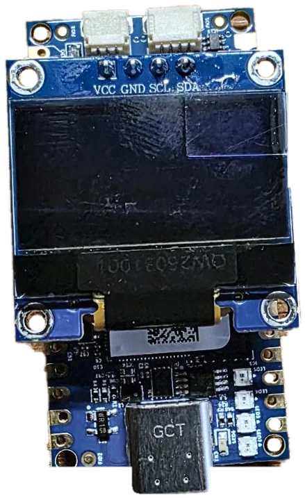
| Display header | 4-pin, 2.54 mm header (VCC · GND · SCL · SDA) on I2C1 for a common 0.96" / 1.3" I²C OLED module, address 0x3C |
| BOOT button | Hold while pressing RESET to start the USB bootloader (see Updating firmware) |
| RESET button | Restarts the module |
| RGB LEDs × 4 | Addressable LEDs, set from the console or scripts with g\s |
| microSD slot (CN3) | On the underside. Storage for scripts, settings and files. The console and API see it as drive 1: |
| BATTERY (CN5) | On the underside. 2-pin connector for a single-cell 3.7 V Li-ion / LiPo battery (see Connecting a battery) |
Bottom side
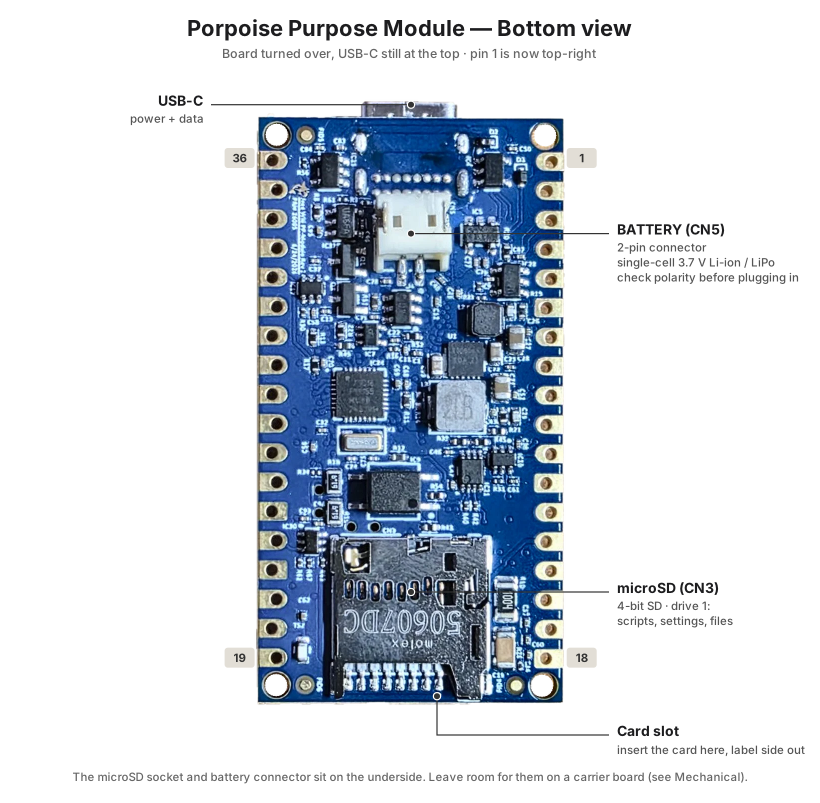
Turned over, the pads are mirrored: pin 1 is at the top-right, next to the USB-C connector.
- microSD (CN3) sits at the end opposite the USB-C connector. Slide the card in from that edge, label side facing out. The firmware creates its settings files and a
/scriptsfolder on first use. Use a card formatted as FAT32 (exFAT is not supported, so format cards over 32 GB as FAT32). - BATTERY (CN5) sits just below the USB-C connector.
Getting started
- Plug in USB-C. The module starts up and appears as a USB serial port (COM port on Windows,
/dev/ttyACM*on Linux,/dev/cu.usbmodem*on macOS). - Open a serial terminal on that port. The baud rate does not matter.
Note: Your terminal must assert DTR. The module stays silent until the host raises DTR. Most terminals (PuTTY, Tera Term,
screen,minicom) do this automatically. Some scripting libraries leave it off by default: .NET'sSerialPortneedsDtrEnable = true. - Press Enter to draw the main menu. The boot banner prints before your terminal connects, so Enter redraws it.
- Set IO VREF if you plan to use the buffered pins (see Setting the I/O voltage).
- Try a few commands:
i\g\s 25          GPIO25 high
i\g\l 25          GPIO25 low
i\g\p 25 1000 50  GPIO25: 1 kHz PWM, 50 % duty
i\g\u             read all GPIO levels (hex)
g\s 0 60 0 0 0 0  RGB LED 0 steady red
Press Ctrl-C at any time to return to the top of the menu.
Console overview
| Path | What it does |
|---|---|
i\g | GPIO: high, low, toggle, PWM, read all, IO directions |
i\u | UART: write, API mode, settings (pins 8–11) |
i\e | SPI: write and read, settings (pins 14–17) |
i\i | I²C: write, poll, bus monitor, settings. Works on I2C0 (pins 4–5), not on the Qwiic bus |
i\c | CAN FD: transmit, periodic frames, stream, filters, receive queue |
i\l | Serial LEDs: drive up to 3 external addressable LED strips on GPIO25 / GPIO26 / GPIO27 |
i\j | Analog in: stream readings from pin 28 (GPIO46) |
g\s | Board LEDs: set LED 0–3 colour and mode (steady, flash, pulse, fades) |
h\a | System: device state and identity |
h\x | Files: browse, transfer and manage the microSD card |
h\s | Settings: UART / I²C / SPI / IO directions / CAN, saved to microSD |
h\p | Power zones: list, get, set |
h\t / h\c | Get / set time: real-time clock |
s\r / s\w | rThon / WiliWasm debuggers |
CAN FD
CAN uses pins 1 (CAN L) and 2 (CAN H), plus a ground pin. Bit rates, mode, listen-only and termination live under h\s\p (CAN channel 0). Settings are applied at start-up, so reboot after changing them.
| Command | Does |
|---|---|
i\c\w | Transmit a CAN or CAN FD frame. Separate data bytes with spaces: DE AD BE EF |
i\c\p | Transmit a frame periodically |
i\c\o | Stream received frames to the console |
i\c\v | Read received frames |
i\c\f | Set up receive filters |
i\c\e | Enable the receive queue |
The CAN transceiver is powered from zone 1 (5V), which is on by default. If CAN stops responding, check that zone 1 is on.
Scripting and the API
rThon and WiliWasm
Scripts run on the module from the microSD card, just as they do on FREE-WILi 2:
runscript hello.rtn     # rThon source (.rtn)
runscript blink.wasm    # WiliWasm bytecode
stopscript              # stop the running script
A fresh microSD card gets a /scripts/hello.rtn example on first use. A script written for FREE-WILi 2's board LEDs runs here unchanged:
dev.gui.set_led_color(0, 60, 0, 0, 0, 0)     # LED 0 steady red
dev.gui.set_led_color(2, 0, 0, 60, 500, 1)   # LED 2 blue, flashing every 500 ms
OneWili API
The module speaks OneWili, the same host API as FREE-WILi 2, over its USB serial port. Every command the two boards share has the same command ID, so host code written for FREE-WILi 2 (Python, Rust, C/C++, rThon) works on the module for UART, SPI, I²C, GPIO, CAN, LEDs, files and power zones. Commands for hardware the module does not have (display, FPGA, radios) fail cleanly rather than doing something unexpected.
See the FREE-WILi Python library and the OneWili API reference.
Updating firmware
With the FREE-WILi GUI (recommended)
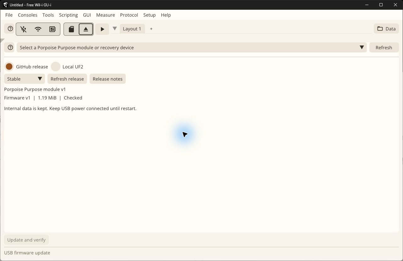
- Connect the module by USB-C and open the FREE-WILi GUI.
- Click the firmware update button (⏏) in the toolbar. The status bar shows USB firmware update.
- In the device list, choose Porpoise Purpose module. Click Refresh if it is not listed.
- Choose the firmware source:
- GitHub release: choose a channel (Stable is recommended), then Refresh release. Release notes shows what changed.
- Local UF2: pick a
.uf2file from your computer.
- Click Update and verify.
Your settings and files are kept. Keep USB connected until the module restarts.
Manual recovery (USB bootloader)
If the module will not start, or does not appear in the GUI:
- Hold BOOT.
- Press and release RESET.
- Release BOOT. A new USB drive appears on your computer.
- Either copy the firmware
.uf2file onto that drive, or pick the module from the GUI's device list. The GUI lists bootloader devices as recovery devices.
The module restarts automatically when the copy finishes.
Mechanical

- Board: 51.00 × 26.00 mm.
- Edge pads: 36 castellated pads, 2.54 mm (0.100") pitch, Ø1.00 mm holes. Rows are 43.18 mm long.
- Header retention: the pads are offset about 0.41 mm along the board, so standard 2.54 mm headers press in and stay put without solder. That works for temporary set-ups. Solder them for anything permanent.
- Mounting: 4 × Ø2.20 mm holes, 22.70 mm apart across the board. They take 2 mm nylon snap-lock spacers (for example Würth Elektronik 709651500, 5 mm height, for 1.2–1.7 mm panels).
- Mounting on a carrier: solder the castellated edges flat onto a matching footprint. The microSD socket and the battery connector are on the underside, so cut a clearance hole in the carrier under them (and leave room to reach the card slot), or raise the module on headers.
Troubleshooting
| Symptom | Check |
|---|---|
| Serial port opens but nothing prints | Your terminal is not asserting DTR. Press Enter to redraw the menu |
| UART / SPI / GPIO pins do nothing | IO VREF (pin 20) is not powered, or the pin's direction is set to input (h\s\o) |
| Buffered I²C (GPIO16/17) does not work | IO VREF is below 3.3 V, or pull-ups are off (h\s\i\p 1) |
| CAN frames are not acknowledged | Zone 1 (5V) is off, termination is missing on a short bus, or the bit rates do not match. Reboot after changing CAN settings |
| A power zone output stays at 0 V | IO VREF is not powered. The zone outputs switch IO VREF |
| Module does not show up for an update | Use manual recovery |
| Console is stuck inside a menu | Press Ctrl-C |