FPGA Default Application

The default FPGA application is a simple design that transforms the FREE-WILi into a sigrok-compatible logic analyzer.
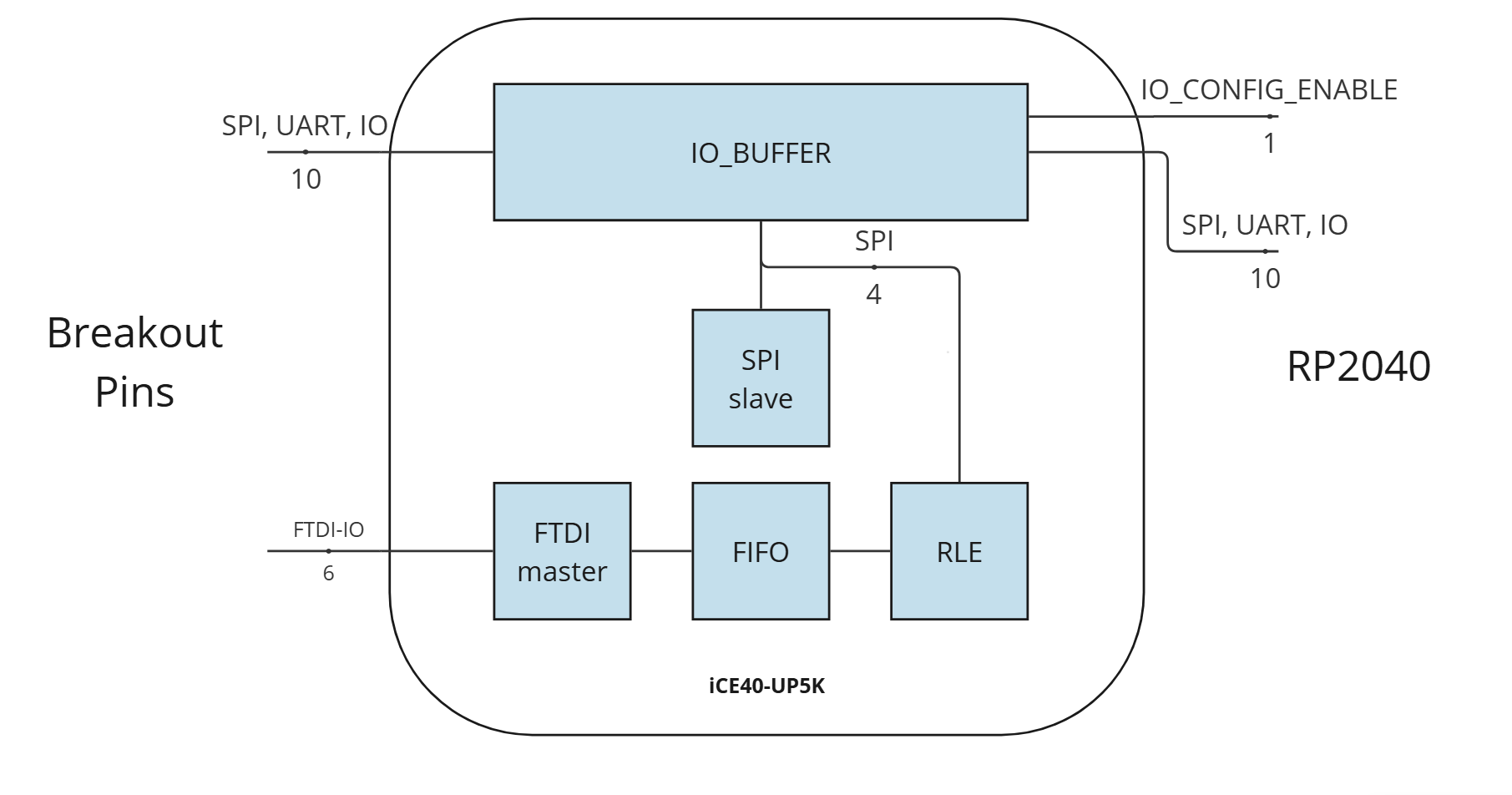
The design features an IO buffer that can set the directions of the SPI and UART pins as well as GPIO_26 and GPIO27. To enable this programming, the IO_CONFIG_ENABLE pin must be asserted - this allows the FPGA's SPI-Slave to assume control of the SPI interface with the main RP2040 as the master. The pin direction defaults are as specified in GPIO. Please note that the pin directionality is also dependent on the sn74lxc1t45 hardware IO buffers between the FPGA and breakout pins.
For the logic analyzer, the FPGA samples the SPI pins at the clock frequency provided by the main RP2040 - this design expects a frequency of 31.25 MHz. The samples are encoded via Run-Length Encoding and, once the FPGA is initiated by sigrok via FTDI, stored in a 32 kB FIFO built using the iCE40's on-chip SPRAM. Finally, these samples are sent via the FT1248 4-wire communication protocol to USB where sigrok can collect them. The libsigrok fork where the FREE-WILi hardware driver was developed can be found at libsigrok-fwili.
The translation from the sigrok channel name to the corresponding pin for SPI protocol is detailed below.
| sigrok channel name | SPI |
|---|---|
| 4 | CS |
| 3 | SCLK |
| 2 | MOSI |
| 1 | MISO |