GPIO Pinout & Electrical Specifications
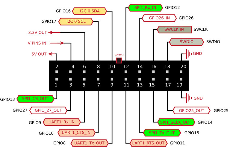
Pinout Diagram
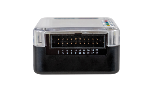
FREE-WILi includes a 20-pin GPIO header with the following layout:


GPIO Pin Descriptions
| Pin | Description | Default Direction | RP2040 GPIO | Buffer Chip | Notes |
|---|---|---|---|---|---|
| 1 | SPI Chip Select Out | Output | GPIO13 | SN74LXC1T45 | |
| 2 | 5V Out | Output | - | - | 5V power output for external circuits |
| 3 | GPIO27 OUT | Output | GPIO27 | SN74LXC1T45 | General purpose I/O |
| 4 | V PINS IN | Input | - | - | REQUIRED: Sets I/O voltage level (1.1V to 5.5V) |
| 5 | UART1 Rx IN | Input | GPIO9 | SN74LXC1T45 | UART receive |
| 6 | 3.3V Out | Output | - | - | 3.3V power output for external circuits |
| 7 | UART1 CTS IN | Input | GPIO10 | SN74LXC1T45 | UART Clear To Send |
| 8 | I2C0 SCL | In/Out | GPIO17 | PCA9517 | I2C clock with software-controlled pullups |
| 9 | UART1 TX OUT | Output | GPIO8 | SN74LXC1T45 | UART transmit |
| 10 | I2C0 SDA | In/Out | GPIO16 | PCA9517 | I2C data with software-controlled pullups |
| 11 | UART1 RTS OUT | Output | GPIO11 | SN74LXC1T45 | UART Request To Send |
| 12 | SPI1 RX IN | Input | GPIO12 | SN74LXC1T45 | SPI receive (MISO) |
| 13 | SPI1 TX OUT | Output | GPIO15 | SN74LXC1T45 | SPI transmit (MOSI) |
| 14 | GPIO 26 IN | Input | GPIO26 | SN74LXC1T45 | General purpose I/O |
| 15 | SPI1 SCLK OUT | Output | GPIO14 | SN74LXC1T45 | SPI clock |
| 16 | SWCLK IN | Input | SWCLK | - | SWD debugger clock input |
| 17 | GPIO25 OUT | Output | GPIO25 | SN74LXC1T45 | General purpose I/O (also board status LED) |
| 18 | SWDIO | In/Out | SWDIO | - | SWD debugger I/O |
| 19 | GND | - | - | - | Ground reference |
| 20 | GND | - | - | - | Ground reference |
Voltage Level Configuration
Critical: Pin 4 (V PINS IN) MUST have a voltage applied for GPIO functionality to work.
Jumper Configuration
- 5V Operation: Connect jumper between pins 2 and 4
- 3.3V Operation: Connect jumper between pins 4 and 6
- Custom Voltage: Apply 1.1V to 5.5V directly to pin 4
The voltage on pin 4 sets the I/O level for all buffered GPIO pins.
Electrical Specifications
Current Drive Capabilities
SN74LXC1T45 Buffered Pins (UART, SPI, GPIO 25/26/27):
- Recommended: 24 mA @ 3.3V, 32 mA @ 5V
- Absolute Maximum: 50 mA (regardless of voltage)
- Voltage Range: 1.1V to 5.5V (set by V PINS IN)
PCA9517 Buffered Pins (I2C):
- Maximum: 50 mA
- Voltage Range: 0.9V to 5.5V (set by V PINS IN)
- Features: Software-controllable 10kΩ pull-up resistors
Power Supply Pins:
- Pin 2 (5V): Up to 3A theoretical maximum (shared with entire system)
- Pin 6 (3.3V): Up to 3A theoretical maximum (shared with entire system)
Buffer Chip Datasheets
SN74LXC1T45 (UART, SPI, GPIO pins):

sn74lxc1t45.pdf
PCA9517 (I2C pins):

PCA9517-3139014.pdf
Pin Direction Control
All GPIO pins can be configured as input or output:
- GUI Method: Use the GPIO panel in the graphical interface on the device
- Serial Console: Navigate to Settings > GPIO Directions
- Important: Settings changes via serial console take effect only after returning to the main menu
Pin directions can be changed dynamically during operation. The RP2040, FPGA, and I/O buffers automatically coordinate direction changes.