GPIO
Overview
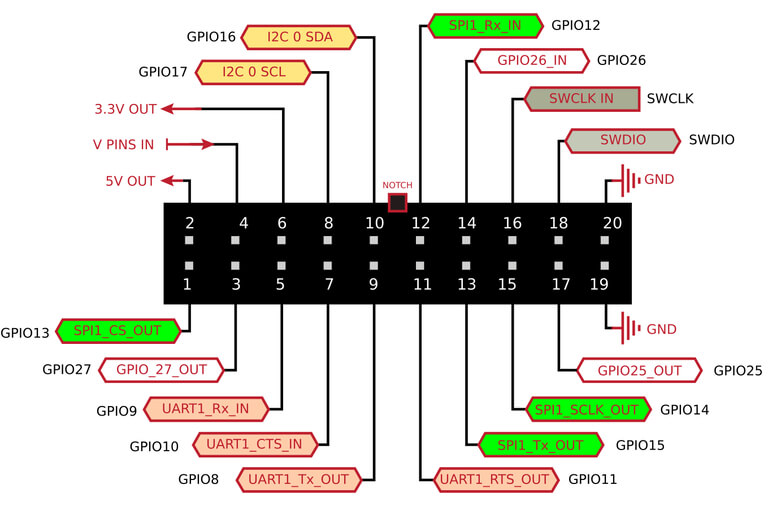
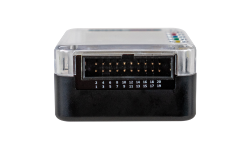
FREE-WILi includes a GPIO pin header for interacting with digital protocols. This GPIO header is flexible, allowing varying voltage levels and IO direction control. The GPIO system supports SPI, I2C, UART, and general-purpose digital I/O operations.


GPIO System Architecture
The GPIO pins are routed through level-shifting buffers and an iCE40UP5K FPGA before connecting to the RP2040 main processor. This architecture enables real-time operations such as the logic analyzer functionality while maintaining protocol compatibility.
Quick Start
- Set I/O Voltage Level: Connect a jumper between pins 2-4 (5V) or 4-6 (3.3V)
- Pin 4 MUST have voltage for GPIO to function
- Configure Pin Directions: Use the GPIO panel in the GUI or settings menu via serial console
- Select Protocol: Access SPI, I2C, or UART functionality through the main console application
GPIO Documentation Sections
- Pinout & Electrical Specifications - Pin descriptions, voltage levels, and electrical characteristics
- Protocol Configuration - SPI, I2C, and UART setup and specifications
- Common Issues & Troubleshooting - Solutions to frequent problems
Related Documentation
- Logic Analyzer - Real-time GPIO monitoring and analysis
- WASM Scripting - Advanced GPIO control through WebAssembly
- ZoomIO Scripting - Nanosecond-precision GPIO timing
- Settings Menu - GPIO direction and protocol configuration